
Footprints
A footprint is a copper area on a circuit board to which a component is soldered. For example, a 16 pin SOIC footprint has two rows of eight rectangular pads. Footprints include the copper layout, layout of solder mask, silkscreen, mounting holes if applicable, and pin attributes.
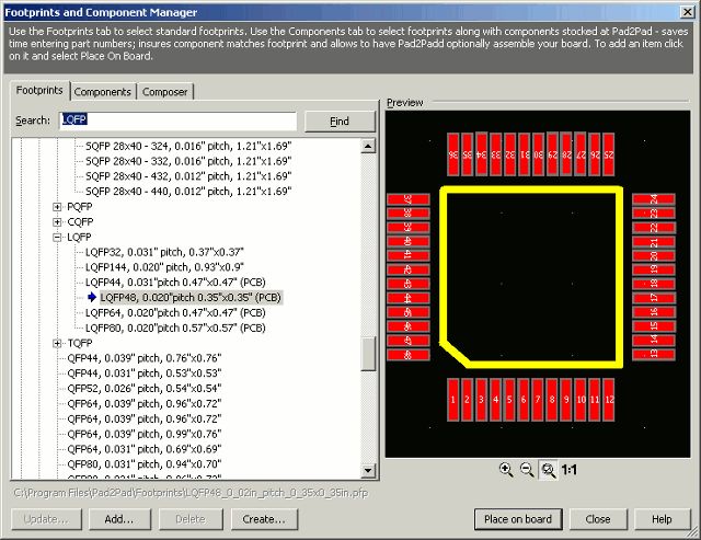
The footprint library is a set of predefined common footprints and custom footprints that you can create. You can view the footprint library to make a selection. For example, you might look for a 16 pin SOIC footprint in the library.
To view the Component Library:
- In the left toolbar select the Footprint/Component tool. A dialog appears.
- Find the desired footprint or component. Use the keyboard arrow keys to browse through the library.
- Click on a footprint or component to get a preview image.
Custom footprints are stored under the My Footprints branch of the footprint tree.
The Pad2Pad footprint library contains a variety of entries including:- SIP (single-in-line package);
- SOJ (single outline J-bent package)
- DIP (dual-in-line package);
- SOP (small outline package);
- QFP (quad flat package);
- LCC (leadless chip carrier);
- BGA (ball grid array);
- And many others.
Examples:
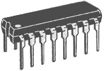
DIP 16 package
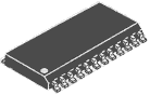
SOP 24 package
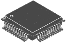
QFP44 package
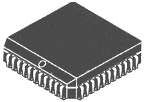
LCC44 package
Placing Footprints or Components
You can place footprints or components anywhere on your design. For example, you could place a resistor footprint or an assembled resistor component next to an Integrated Circuit.
To place a footprint:
- On the property bar click Layers and choose Top or Bottom.
- On the left toolbar select the Footprint/Component tool. A dialog box appears.
- Select the Footprint tab or if you want to place an assembled component, use the Component tab.
- Select an item or use the Search box and click Find.
- Click Place on board.
- Press the R key to Rotate the item if needed.
- Position the mouse at the desired footprint location.
- Left click to place the item.
- Right click if no additional copies of the item are needed.
Custom Footprints
A custom footprint is a footprint that you design – generally because it does not already exist in the footprint library. You can create your own custom footprints and add them to the library. For example, you might need a custom footprint for an exotic connector you plan to use.
You can create a custom footprint manually by creating pads, silkscreen legends, etc.
You can add a custom footprint to the library to allow convenient selection in future designs.
To create a custom footprint manually:
You can create a new footprint based on an existing footprint.
- Add the appropriate pad layout and other features (e.g. silk screen) to your design. To add pads use the pad tool or the multilayer padtool.
- Group the elements together using the Make a footprint option.
- Cut and paste as needed.
To create a custom footprint based on an existing footprint:
You can create a footprint using a wizard for DIP, SIP, SO, BGA, QFP and Tabbed devices.
- Place the existing footprint.
- Select the footprint and choose Edit | Ungroup.
- Edit the footprint to add mounting holes, modify silkscreen, change pad layout, re-number pads, etc.
- Group the elements together.
- Cut and paste as needed.
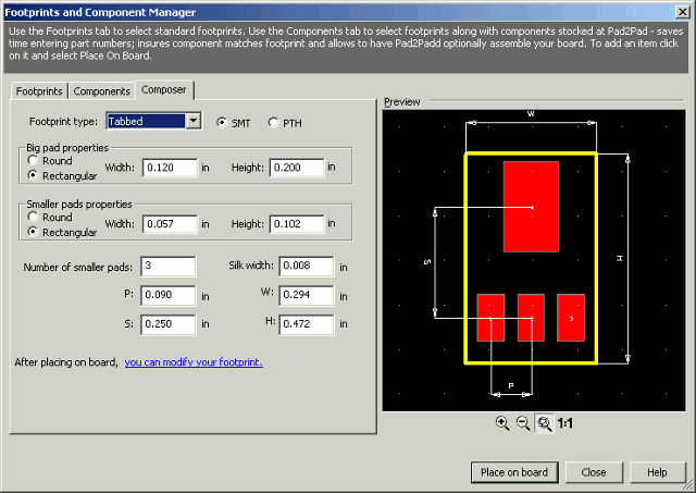
To create a custom DIP, SIP, SO, BGA, QFP or Tabbed footprint:
- Review the component manufacturer’s drawing of the component, noting the relevant dimensions.
- On the left toolbar select the Footprint / Component tool. A dialog appears.
- Select the Composer tab.
- Choose an appropriate footprint type.
- Enter the footprint parameters and dimensions.
- Click Place on board.
- To edit your footprint, follow “To create a custom footprint based on an existing footprint” above starting from the step 2.
You can add a custom footprint to the library to allow convenient selection in future designs.
To add your custom footprint to the Component Library
To edit your custom footprint just open the footprint file located in your custom footprints folder, make changes, and save.
- If your footprint is saved alone in a separate .pcb file, skip to step 10.
- Select your footprint and choose Edit | Copy.
- Choose File | New
- Click OK.
- Choose Edit | Select | All.
- Choose Edit | Delete.
- Choose Edit | Paste.
- Choose File | Save select your custom footprints folder and enter a meaningful name for your footprint file. You can organize your footprints into sub-folders.
- Choose File | Close.
- In the left toolbar select the Footprint / Component tool. A dialog appears.
- Select your custom footprints folder by clicking the “…” button at the “My footprints directory” edit box.
- Your footprint will appear under the My Footprints branch of the footprint tree.
Replace footprints
To propagate changes made to a footprint to other footprints that are already on board:
- Select a footprint with changes to be propagated*.
- Choose Tools | Replace footprints. The command is also on the context menu.
- Replace Footprints dialog appears.
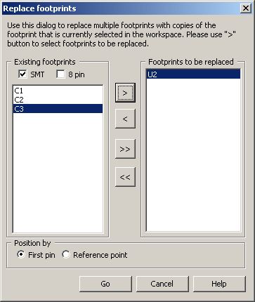
- Add footprints to be replaced to the right column.
- Click “Go“
Please make sure your footprint has not been rotated before grouping otherwise replaced footprints will appear rotated. Please don’t make changes to a footprint that is already on board when traces are connected. It’s recommended to make a copy of your footprint and then make changes to the copy. Before ungrouping the copy make sure it’s not rotated.