
Plated through slots
To draw a plated through slot:
- Use the trace tool on the board layer to draw the contour of your slot. The slot width should not be below 0.8mm (0.032″)

- Put multilayer pads at each end of the slot:

- Use the trace tool to draw copper traces on the top and bottom layers. The width of the traces must be equal to the pad diameter.
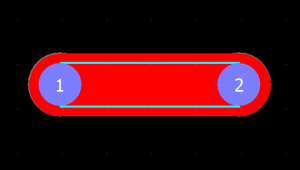
- Right click each trace and select Unmask to make the slot completely clear of solder mask to allow soldering:
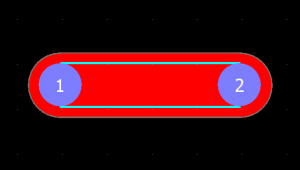
- Select all slot elements and choose Edit | Group | Simply group items together.
To draw a square plated-through hole:
- Basically follow the slot instruction except put multilayer pads at each corner of the hole. The multilayer pad hole diameter should not be below 0.8mm (the min fillet radius is 0.4mm)
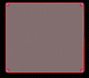
Ignore analyzer board outline intersect/overlap warnings relating to the slot.
Edge connector
Follow the below steps to add an edge connector to your board.
- Make sure “Paste at mouse cursor” is unchecked at Edit | Preferences | General
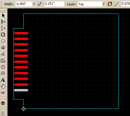
- Use the Trace tool to draw the 1st finger of the connector.
- Enter the finger pitch into the nudge linear step field on the toolbar.
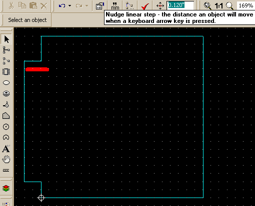
- Select the 1st finger.
- Press Ctrl+C to copy, Ctrl+V to paste to make the next finger.
- Press the left arrow key to position the new finger into the place.
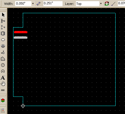
- Repeat the above 2 steps until all of the fingers are added.
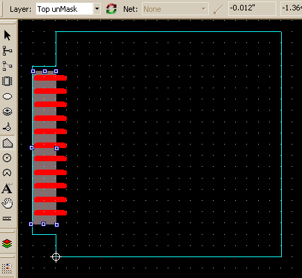
- Select the Polygon tool, select the Top unMask layer on the property bar and draw a polygon over the fingers to make them open for contact.
If gold plating required, please check the “Gold fingers or gold plating required…” checkbox in Job | Settings | Specifications | Advanced settings.